Power Electronics – Introduction
Power Electronics refers to the process of controlling the flow of current and voltage and converting it to a form that is suitable for user loads. The most desirable power electronic system is one whose efficiency and reliability is 100%.
Take a look at the following block diagram. It shows the components of a Power Electronic system and how they are interlinked.
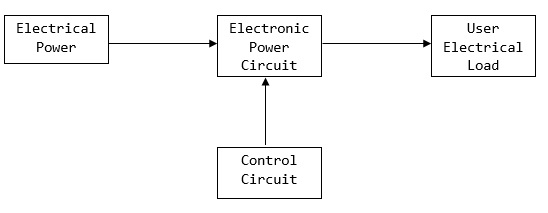
A power electronic system converts electrical energy from one form to another and ensures the following is achieved −
- Maximum efficiency
- Maximum reliability
- Maximum availability
- Minimum cost
- Least weight
- Small size
Applications of Power Electronics are classified into two types − Static Applications and Drive Applications.
Static Applications
This utilizes moving and/or rotating mechanical parts such as welding, heating, cooling, and electro-plating and DC power.
DC Power Supply

Drive Applications
Drive applications have rotating parts such as motors. Examples include compressors, pumps, conveyer belts and air conditioning systems.
Air Conditioning System
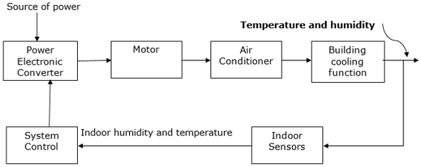
Power electronics is extensively used in air conditioners to control elements such as compressors. A schematic diagram that shows how power electronics is used in air conditioners is shown below.
Power Electronics – Switching Devices
A power electronic switching device is a combination of active switchable power semiconductor drivers that have been integrated into one. The main characteristics of the switch are determined by internal correlation of functions and interactions of its integrated system. The figure given below shows how a power electronic switch system works.
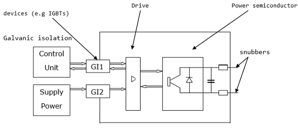
The external circuit of the above diagram is usually held at a high potential relative to the control unit. Inductive transmitters are used to support the required potential difference between the two interfaces.
Power switching devices are normally selected based on the rating at which they handle power, that is, the product of their current and voltage rating instead of their power dissipation rate. Consequently, the major attractive feature in a power electronic switch is its capability to dissipate low or almost no power. As a result, the electronic switch able to achieve a low and continuous surge of power.
Power Electronics – Linear Circuit Elements
Linear circuit elements refer to the components in an electrical circuit that exhibit a linear relationship between the current input and the voltage output. Examples of elements with linear circuits include −
- Resistors
- Capacitors
- Inductors
- Transformers
To get a better understanding of linear circuit elements, an analysis of resistor elements is necessary.
Resistors
A resistor is a device in which the flow of an electric current is restricted resulting in an energy conversion. For example, when electricity flows through a light bulb, the electricity is converted into a different form of energy such as heat and/or light. The resistance of an element is measured in ohms (Ω).
The measure of resistance in a given circuit is given by −
$$R=rho frac{L}{A}$$
Where R − resistance; ρ − resistivity; L − length of wire; and A − cross-sectional area of wire
Symbol of Various Resistors
| Resistor |  |
| A variable resistor | 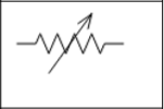 |
| A potentiometer |  |
Capacitors
A capacitor refers to an electrical device that has two conducting materials (also known as plates) separated by an insulator known as a dielectric. It uses electric field to store electric energy. The electric field is developed when the capacitor is connected to a battery, thus making positive electric charges accumulate on one plate and negative electric charges on the other plate.
When energy is stored in the electrical field of a capacitor, the process is called charging, and when energy is removed, the process is called discharging. The level of electrical energy stored in a capacitor is called capacitance and is measured in farads (F). One farad is the same as one coulomb per unit volt given by 1 C/V.
The difference between a capacitor and a battery is that a capacitor stores electrical energy while a battery stores chemical energy and releases the energy at a slow rate.
Symbol of Various Capacitors
The various symbols of a capacitor are given in the table below.
| Fixed Capacitor |  |
| Variable Capacitor |  |
| Polarized Capacitor |  |
Inductors
Inductors are electronic devices that use magnetic field to store electric energy. The simplest form of an inductor is a coil or a wire in loop form where the inductance is directly proportional to the number of loops in the wire. In addition, the inductance depends on the type of material in the wire and the radius of the loop.
Given a certain number of turns and radius size, only the air core can result in the least inductance. The dielectric materials, which serve the same purpose as air include wood, glass, and plastic. These materials help in the process of winding the inductor. The shape of the windings (donut shape) as well as ferromagnetic substances, for example, iron increase the total inductance.
The amount of energy that an inductor can store is known as inductance. It is measured in Henry (H).
Symbol of Various Inductors
| Fixed inductor |  |
| Variable inductor |  |
Transformers
This refers to a device that alters energy from one level to another through a process known as electromagnetic induction. It is usually used to raise or lower AC voltages in applications utilizing electric power.
When the current on the primary side of the transformer is varied, a varied magnetic flux is created on its core, which spreads out to the secondary windings of the transformer in form of magnetic fields.
The operation principle of a transformer relies on Faraday’s law of electromagnetic induction. The law states that the rate of change of the flux linking with respect to time is directly related to the EMF induced in a conductor.
A transformer has three main parts −
- Primary winding
- Magnetic core
- Secondary winding
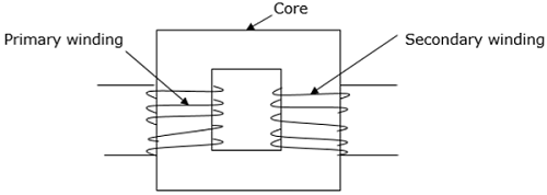
Symbol of a Transformer

Additional Devices
Electromagnetic Devices
The concept of electromagnetism is widely used in technology and it is applied in motors, generators and electric bells. For example, in a doorbell, the electromagnetic component attracts a clapper that hits the bell and causes it to ring.
Controllers
Controllers are devices that receive electronic signals transferred from a measured variable in a process and compare the value obtained with a set point of control. It utilizes digital algorithms to correlate and compare functions.
Sensors
Sensors are used to determine current, which constantly varies to provide feedback for purposes of control. Sensing current makes it possible to achieve a smooth and accurate converter function. Current sensors are critical in converters such that the information in parallel or multiphase converters is easily shared.
Filters
Electronic filters are also used to carry out processing of signals to remove undesired frequencies. They are analog circuits and exist in either active or passive state.
Silicon Controlled Rectifier
A silicon controlled rectifier or semiconductor-controlled rectifier is a four-layer solidstate current-controlling device. The name “silicon controlled rectifier” is General Electric”s trade name for a type of thyristor.
SCRs are mainly used in electronic devices that require control of high voltage and power. This makes them applicable in medium and high AC power operations such as motor control function.
An SCR conducts when a gate pulse is applied to it, just like a diode. It has four layers of semiconductors that form two structures namely; NPNP or PNPN. In addition, it has three junctions labeled as J1, J2 and J3 and three terminals(anode, cathode and a gate). An SCR is diagramatically represented as shown below.
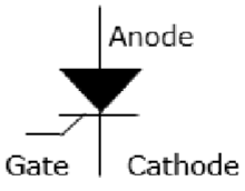
The anode connects to the P-type, cathode to the N-type and the gate to the P-type as shown below.
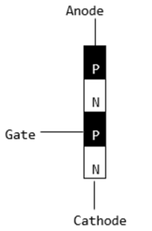
In an SCR, the intrinsic semiconductor is silicon to which the required dopants are infused. However, doping a PNPN junction is dependent on the SCR application.
Modes of Operation in SCR
-
OFF state (forward blocking mode) − Here the anode is assigned a positive voltage, the gate is assigned a zero voltage (disconnected) and the cathode is assigned a negative voltage. As a result, Junctions J1 and J3 are in forward bias while J2 is in reverse bias. J2 reaches its breakdown avalanche value and starts to conduct. Below this value, the resistance of J1 is significantly high and is thus said to be in the off state.
-
ON state (conducting mode) − An SCR is brought to this state either by increasing the potential difference between the anode and cathode above the avalanche voltage or by applying a positive signal at the gate. Immediately the SCR starts to conduct, gate voltage is no longer needed to maintain the ON state and is, therefore, switched off by −
-
Decreasing the current flow through it to the lowest value called holding current
-
Using a transistor placed across the junction.
-
Reverse blocking − This compensates the drop in forward voltage. This is due to the fact that a low doped region in P1 is needed. It is important to note that the voltage ratings of forward and reverse blocking are equal.
Power Electronics – TRIAC
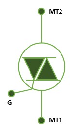
The acronym TRIAC stands for Triode for Alternating Current. A TRIAC is a semiconductor device with three terminals that control the flow of current, thus the name Triac. Unlike SCR, TRIAC is bi-directional while SCR is bi-directional. It is ideal for operation utilizing AC power for switching purposes since it can control current flow for both halves in an alternating current cycle. This explained clearly in the diagram below.
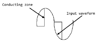
TRIAC Symbol
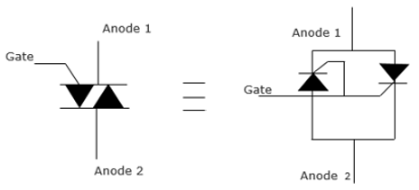
The circuit diagram for a TRIAC is shown below. It resembles two thyristors placed back to back.
TRIAC Structure
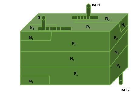
The TRIAC Structure is regarded as a DIAC having an extra gate contact incorporated to ensure device control. Similar to other power devices, the TRIAC is manufactured from silicon. Consequently, the process of fabricating the silicon leads to the production of cheaper devices. As indicated below, the TRIAC has a six areas namely; four N-type regions and two P-type regions.
TRIAC Operation
The operation of the TRIAC is based on the thyristor. It facilitates the switching function in AC electrical components and systems. They are widely used in light dimmers because they allow both halves of the AC cycle to be utilized. As a result, this makes them more efficient in power usage. As much as it is possible to use thyristors to function as TRIAC, it is not cost efficient for operations that require low power. It is possible to view a TRIAC in terms of two thyristors.
TRIACs are normally used in applications that do not require very high power because they exhibit non-symmetrical switching in their operation. This is disadvantageous for applications utilizing high power as it causes electromagnetic interference. As a result, TRIACs are used in motor controls, light residential light dimmers and small electric fans to control speed.
Power Electronics – BJT
A Bipolar Junction Transistor (BJT) is a transistor whose operation depends on the contact made by two semicondutors. It can act as a switch, amplifier or oscillator. It is known as a bipolar transistor since its operation requires two types of charge carriers (holes and electrons). Holes constitute the dominant charge carriers in P-type semiconductors while electrons are the main charge bearers in N-type semiconductors.
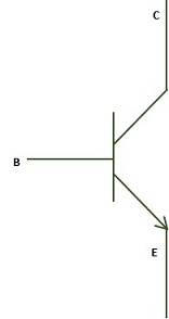
Symbols of a BJT
Structure of a BJT
A BJT has two P-N junctions connected back to back and sharing a common region B (base). This ensures contacts are made in all the regions that are base, collector and emitter. The structure of a PNP bipolar transistor is shown below.
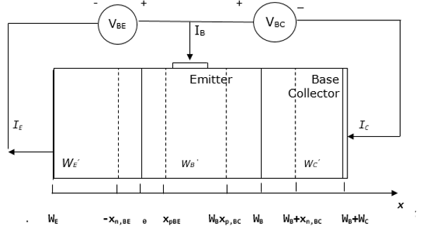
The BJT shown above consists of two diodes connected back to back, resulting in the depletion of the regions called quasi-neutral. The width of quasi-neutral of the emitter, base and collector are indicated above as WE’, WB’ and WC’. They are obtained as follows −
$$W_{E}^{”}=W_{E}-X_{n,BE}$$
$$W_{B}^{”}=W_{B}-X_{p,BE}-X_{p,BC}$$
$$W_{C}^{”}=W_{C}-X_{n,BC}$$
The conventional signs of the currents for the emitter, base and collector are denoted by IE, IB and IC respectively. Therefore, the collector and base current are positive when a positive current meets the collector or base contact. In addition, the emitter current is positive when current leaves the emitter contact. Thus,
$$I_{E}=I_{B}+I_{C}$$
When a positive voltage is applied to the base contact relative to the collector and emitter, the base-collector voltage as well as base-emitter voltage becomes positive.
For simplicity, VCE is assumed to be zero.
Diffusion of electrons occur from the emitter to the base while diffusion of holes originates from the base to the emitter. Once the electrons reach the base-collector depleted region, they are swept through the region by an electric field. These electrons form the collector current.
When a BJT is biased in the forward active mode, the total emitter current is obtained by adding the electron diffusion current (IE,n), the hole diffusion current (IE, p) and the baseemitter current.
$$I_{E}=I_{E,n}+I_{E,p}+I_{r,d}$$
The total collector current is given by the electron diffusion current (IE,n), less the base recombination current(Ir,B).
$$I_{C}=I_{E,n}-I_{r,B}$$
The sum of the base current IB is obtained by adding the hole diffusion current (IE, p), base recombination current (Ir,B) and the base-emitter recombination current of the depletion layer (Ir,d).
$$I_{B}=I_{E,p}+I_{r,B}+I_{r,d}$$
Transport Factor
This is given by the ratio of the collector current and the emitter current.
$$alpha =frac{I_{C}}{I_{E}}$$
Applying the Kirchhoff’s current law, it is found that the base current is given by the difference between the emitter current and the collector current.
Current Gain
This is given by the ratio of the collector current to the base current.
$$beta =frac{I_{C}}{I_{B}}=frac{alpha }{1-alpha }$$
The above explains how a BJT can produce current amplification. The transport factor (α) approaches one if the collector current is almost equivalent to the emitter current. The current gain (β) thus becomes greater than one.
For further analysis, the transport factor (α) is rewritten as a product of the emitter efficiency (γE) the base transport factor (αT) and the recombination factor of the depletion layer (δr). It is rewritten as follows −
$$alpha =gamma _{E}times alpha _{T}times delta _{r}$$
The following is a summary of the discussed emitter efficiency, base transport factor and depletion layer recombination factor.
Emitter Efficiency
$$gamma _{E}=frac{I_{E,n}}{I_{E,p}+I_{E,P}}$$
Base Transport Factor
$$alpha _{T}=frac{I_{E,n}-I_{r,b}}{I_{E,n}}$$
Depletion Layer Recombination Factor
$$delta _{r}=frac{I_{E}-I_{r,d}}{I_{E,n}}$$
Power Electronics – IGBT
The insulated gate bipolar transistor (IGBT) is a semiconductor device with three terminals and is used mainly as an electronic switch. It is characterized by fast switching and high efficiency, which makes it a necessary component in modern appliances such as lamp ballasts, electric cars and variable frequency drives (VFDs).
Its ability to turn on and off, rapidly, makes it applicable in amplifiers to process complex wave-patterns with pulse width modulation. IGBT combines the characteristics of MOSFETs and BJTs to attain high current and low saturation voltage capacity respectively. It integrates an isolated gate using FET (Field effect transistor) to obtain a control input.
IGBT Symbol
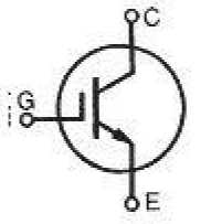
The amplification of an IGBT is computed by the ratio of its output signal to its input signal. In conventional BJTs, the degree of gain (β) is equal to the ratio of its output current to the input current.
IGBT has a very low value of ON state resistance (RON) than a MOSFET. This implies that the voltage drop (I2R) across the bipolar for a particular switching operation is very low. The forward blocking action of the IGBT is similar to that of a MOSFET.
When an IGBT is used as controlled switch in a static state, its current and voltage ratings equal to that of BJT. On the contrary, the isolated gate in IGBT makes it easier to drive BJT charges and hence less power is required.
IGBT is switched ON or OFF based on whether its gate terminal has been activated or deactivated. A constant positive potential difference across the gate and the emitter maintains the IGBT in the ON state. When the input signal is removed, the IGBT is turned OFF.
IGBT Principle of Operation
IGBT requires only a small voltage to maintain conduction in the device unlike in BJT. The IGBT is a unidirectional device, that is, it can only switch ON in the forward direction. This means current flows from the collector to the emitter unlike in MOSFETs, which are bi-directional.
Applications of IGBT
The IGBT is used in medium to ultra-high power applications, for example traction motor. In large IGBT, it is possible to handle high current in the range of hundred amperes and blocking voltages of up to 6kv.
IGBTs are also used in power electronic devices such as converters, inverters and other appliances where the need for solid state switching is necessary. Bipolars are available with high current and voltage. However, their switching speeds are low. On the contrary, MOSFETs have high switching speeds although they are expensive.
Power Electronics – MOSFET
Metal Oxide Semiconductor Field Effect Transistor (MOSFET) is a type of transistor used to switch electronic signals. It has four terminals namely; source (S), Drain (D), Gate (G) and Body (B).The MOSFET’s body is normally connected to the terminal of the source(S), which results in three-terminal device similar to other field effect transistors (FET). Since these two main terminals are usually interconnected via short circuit, only three terminals are visible in electrical diagrams.
It is the most common device in circuits that are both digital and analogue. Compared to the regular transistor, a MOSFET needs low current (less than one mill-ampere) to switch ON. At the same time, it delivers a high current load of more than 50 Amperes.
Operation of a MOSFET
MOSFET has a thin layer of silicon dioxide, which acts as the plate of a capacitor. The isolation of the controlling gate raises the resistance of the MOSFET to extremely high levels (almost infinite).
The gate terminal is barred from the primary current pathway; thus, no current leaks into the gate.
MOSFETs exist in two main forms −
-
Depletion state − This requires the gate-source voltage (VGB) to switch the component OFF. When the gate is at zero (VGB) the device is usually ON, therefore, it functions as a load resistor for given logic circuits. For loading devices with N-type depletion, 3V is the threshold voltage where the device is switched OFF by switching the gate at negative 3V.
-
Enhancement state − The gate-source voltage (VGB) is required in this state to switch the component ON. When the gate is at zero (VGB) the device is usually OFF and can be switched ON by ensuring the gate voltage is higher than the source voltage.
Symbol and Basic Construction
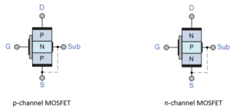
Where, D − Drain; G − Gate; S − Source; and Sub − Substrate
Power Semiconductor Devices Solved Ex
A (BJT) emits a current of 1mA, and has emitter efficiency of 0.99. The base transport factor is 0.994 and a depletion layer recombination factor is 0.997. For the BJT calculate the following −
The transport factor
The rewritten transport factor is given by −
$$alpha =gamma _{E}times alpha _{T}times delta _{r}$$
Substituting the values, we get
$$alpha =0.99times 0.994times 0.997=0.981$$
The current gain
Current gain is given by −
$$beta =frac{I_{C}}{I_{B}}=frac{alpha }{1-alpha }$$
Substituting the values, we get
$$beta =frac{0.981}{1-0.981}=51.6$$
The collector current
$$I_{C}=alpha times I_{E}=0.981times 1=0.981mA$$
The base current
$$I_{B}=I_{E}-I_{C}=1-0.981=19mu A$$
Power Electronics – Pulse Converters
Phase Controlled Converter
A phase controlled converter converts AC to DC energy (line commutated). In other words, it is used in the conversion of fixed-frequency and fixed-voltage AC power into variable DC voltage output. It is expressed as
-
Fixed Input − Voltage, frequency and AC power
-
Variable output − DC voltage output

The AC input voltage that goes into a converter is normally at fixed RMS (root mean square) and fixed frequency. The inclusion of phase-controlled thyristors in the converter ensures that a variable DC output voltage is obtained. This is made possible by altering the phase angle at which the thyristors are triggered. As a result, a pulsating waveform of the load current is obtained.
During the input supply half cycle, the thyristor is in forward bias and is switched ON via the application of sufficient gate pulse (trigger). Current starts to flow once the thyristor has been switched ON, that is, at a point ωt=α to point ωt=β. The moment the load current drops to zero, the thyristor switches OFF as a result of line (natural) commutation.
There are a number of power converters that utilize natural commutation. These include −
- AC to DC converters
- AC to AC converters
- AC voltage controllers
- Cycloconverters
The above power converters will be explained in the next chapters in this tutorial.
2- Pulse Converter
A 2-phase pulse converter, also known as a level 2 pulse width modulator (PWM) generator, is used to generate pulses for pulse width modulation converters that are carrier based. It does this by utilizing level-two topology. This block controls switching devices for control purposes like IGBTs and FETs that exist in three types of converters namely −
- 1 arm (single phase half bridge)
- 2 arms (single phase full bridge)
- 3 arms ( three phase bridge)
The reference input signal in a 2-pulse converter is compared to a carrier. If the reference input signal is more than the carrier, the pulse equals to 1 for the upper device and 0 for the lower device.
In order to control a device with a single-phase full bridge (2 arms), it is necessary to apply unipolar or bipolar pulse width modulation. In unipolar modulation each of the two arms is independently controlled. A second reference input signal is generated internally through a shift in initial reference point by 180°
When the bipolar PWM is applied, the state of the lower switching device in the second single phase full bridge is similar to the upper switch in the first single phase full bridge device. Using a unipolar modulation leads to smooth AC waveforms while the bipolar modulation results in less varying voltage.
3-Pulse Converter
Consider a three-phase 3-pulse converter, where each of the thyristor is in conduction mode during the third of the supply cycle. The earliest time a thyristor is triggered into conduction is at 30° in reference to the phase voltage.
Its operation is explained using three thyristors and three diodes. When the thyristors T1, T2 and T3 are replaced by diodes D1, D2 and D3, conduction will begin at angle 30° in respect to the phase voltages uan, ubn and ucn respectively. Therefore, the firing angle α is measured initially at 30° in reference to the phase voltage corresponding to it.
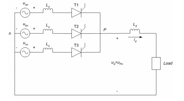
The current can only flow in one direction through the thyristor, which is similar to inverter mode of functioning where power flows from the DC side to the AC side. In addition, the voltage in the thyristors is controlled by controlling the firing angle. This is achieved when α = 0(possible in a rectifier). Thus, the 3-pulse converter acts as an inverter and a rectifier.
6-Pulse Converter
The figure below shows a six-pulse bridge controlled converter connected to a three-phase source. In this converter, the number of pulses is twice that of phases, that is p = 2m. Using the same converter configuration, it is possible to combine two bridges of the six-pulse to obtain a twelve or more pulses converter.
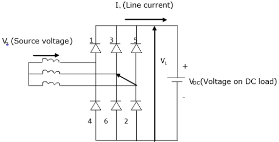
When commutation is not available, two diodes will conduct at any particular time. Furthermore, to obtain a voltage drop across the load, two diodes must be at positioned at opposite legs of the bridge. For example, diodes 3 and 6 cannot be ON at the same time. Therefore, the voltage drop across the DC load is a combination of line voltage VL from the three-phase source.
It is important to note that more the number of pulses, the greater the utilization of the converter. In addition, the fewer the number of pulses the lesser the utilization of the converter.
Effect of Source Inductance
The analysis of most converters is usually simplified under ideal conditions (no source impedance). However, this assumption is not justified since source impedance is normally inductive with a negligible resistive element.
Source inductance has a significant impact on the converter performance because its presence alters the output voltage of the converter. As a result, the output voltage reduces as the load current reduces. In addition, the input current and output voltage waveforms change significantly.
Source inductance effect on a converter is analyzed in the following two ways.
Effect on Single Phase
Assuming that the converter operates in conduction mode and the ripple from the load current is negligible, the open circuit voltage becomes equal to average DC output at a firing angle of α.The diagram below shows a fully controlled converter with source in single phase. The thyristors T3 and T4 are assumed to be in conduction mode when t = 0. On the other hand, T1 and T2 fire when ωt = α
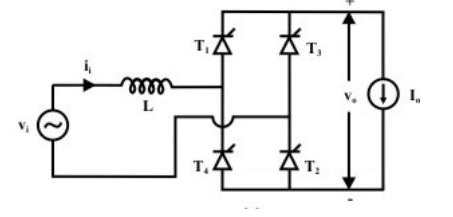
Where −
- Vi = input voltage
- Ii = input current
- Vo = output voltage
- Io = output voltage
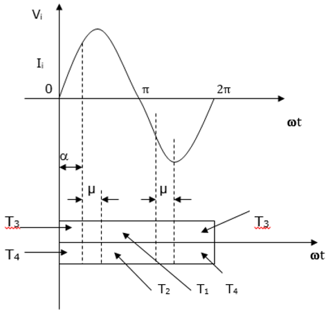
When there is no source inductance, commutation will occur at T3 and T4. Immediately thyristors T1 and T2 are switched ON. This will lead the input polarity to change instantaneously. In the presence of source inductance, change of polarity and commutation does not occur instantaneously. Thus, T3 and T4 do not commutate as soon as T1 and T2 are switched ON.
At some interval, all the four thyristors will be conducting. This conducting interval is called the overlap interval (μ).
The overlap during commutation reduces the DC output voltage and the angle of extinction γ resulting in failed commutation when αis close to 180°. This is shown by the waveform below.
Effect on Three Phase
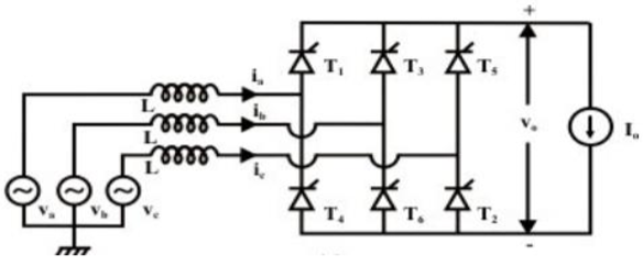
Just like the single-phase converter, there are no instantaneous commutations due to the presence of the source inductances. Taking the source inductances into consideration, the effects (qualitative) on the converter performance is the same as in a single phase converter. This is shown in the diagram below.
Power Electronics – Performance Parameters
It is important to determine the performance parameters for different converters whose topologies can be single phase or multi-phase.
Assumptions
- The devices used are ideal, that is, they do not have any losses
- The devices have resistive loads

DC Voltage on Load
$$V_{DC}=frac{1}{T} int_{0}^{T}V_{L}left ( t right )dt$$
RMS Voltage on Load
$$V_{L}=sqrt{frac{1}{T}}int_{0}^{T}V_{L}^{2}left ( t right )dt$$
Form Factor
$$FF=frac{V_{L}}{V_{DC}}$$
Ripple Factor
$$RF=frac{sqrt{V_{L}^{2}-V_{DC}^{2}}}{V_{DC}}=sqrt{FF^{2}-1}$$
Efficiency(Rectification Factor)
$$eta =frac{P_{DC}}{P_{L}+P_{D}}$$
Where the above are defined as −
$P_{DC}=V_{DC}times I_{DC}$
$P_{L}=V_{L}times I_{L}$
$P_{D}=R_{D}times I_{L}^{2}$($P_{D}$ is the rectifier losses and $R_{D}$ the resistance)
$$eta =frac{V_{DC}I_{DC}}{left ( V_{L}I_{L} right )+left ( R_{D}I_{L}^{2} right )}=frac{V_{DC}^{2}}{V_{L}^{2}}times frac{1}{1+frac{R_{D}}{R_{L}}}$$
But $R_{D}=0$
Therefore,
$$eta =left ( frac{V_{DC}}{V_{L}} right )^{2}=left ( frac{1}{FF}right )^{2}$$
Transformer Utilization Factor
$$TUF=frac{P_{DC}}{VA :Rating :of :the :Transformer
}=frac{P_{DC}}{frac{VA_{p}+VA_{s}}{2}}$$
VAp and VAs are the primary and secondary power ratings of the transformer.
Reactive Power Control of Converters
In high voltage direct current (HVDC) converters, the stations are line commutated. This implies that the initial current of the valve can only be delayed in reference a zero value of the converter bus voltage in AC form. Consequently, for better control of voltage, the converter bus is connected to a reactive power source.
Reactive power sources are used to vary capacitors in static systems. The response of the reactive power system is dictated by voltage control in dynamic conditions.
When operating unstable AC systems, problems tend to arise because of unstable voltage and overvoltage surges. A better coordination of reactive power sources is required to simplify the control of the firing angles. As a result, this feature of the reactive power converter is increasingly being applied in modern converters using HVDC.
Reactive Power Control in Steady State
The equations expressing reactive power as a function of active power are given in terms of unit quantities.
Base converter voltage is given by −
$$V_{db}=3sqrt{frac{2}{pi }}times V_{L}$$
Where VL = Line to line voltage (on winding side)
Base DC Current (Idb ) = Rated DC Current (Idr)
Base DC Power (Pdc) = nb × Vdb × Idb, where nb = number of bridges in series
BaseBase AC voltage (Vb) = (Va)
Base AC Power = Base DC Power
$$sqrt{frac{18}{pi }}times V_{a}times I_{db}times n_{b}$$
Power Electronics – Dual Converters
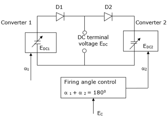
Dual converters are mainly found in variable speed drives (VFDs). In a dual converter, two converters are linked together back to back. The operation of a dual converter is explained using the diagram below. It is assumed that −
-
A dual converter is an ideal one (gives pure DC output) at its terminals.
-
Each two-quadrant converter is a controlled DC source in series with a diode.
-
Diodes D1 and D2 show the unidirectional flow of current.
Considering a dual converter operating without circulating current, the AC current is barred from flowing by controlled firing pulses. This ensures that the converter carrying the load current conducts while the other converter is blocked. This means that a reactor between the converters is not needed.
Battery Charger
A battery charger also known as a recharger utilizes electric current to store energy in a secondary cell. The charging process is determined by the type and size of the battery. Different types of batteries have different tolerance levels to overcharging. The recharging process may be achieved by connecting it to a constant voltage or constant current source.
Charging Rate (C)
The charging rate is defined as the rate of charging or discharging a battery and is equal to the battery capacity in one hour.
A battery charger is specified in terms of its charging rate C. For example, a battery charger with a rating of C/10 would give a charging capacity in 10 hours while one rated 3C would charge a battery in 20 minutes.
Types of Battery Chargers
There are many types of battery chargers. In this tutorial, we will consider the five main types.
-
Simple chargers − Operates by supplying a constant DC power source into the battery being charged.
-
Fast chargers − Uses control circuitry to charger the battery rapidly and in the process prevent the battery cells from damage.
-
Inductive chargers − Uses electromagnetic induction to charge the battery.
-
Intelligent chargers − Used to charge a battery that contains a chip that communicates with the smart charger.
-
Motion powered charger − Makes use of human motion to charge a battery. A magnet placed between two springs is moved up and down by human motion thus charging the battery.
Phase Controlled Converters Solved Example
A separately excited DC motor has the following parameters: 220V, 100A and 1450 rpm. Its armature has a resistance of 0.1 Ω. In addition, it is supplied from a 3 phase fullycontrolled converter connected to a 3-phase AC source with a frequency of 50 Hz and inductive reactance of 0.5 Ω and 50Hz. At α = 0, the motor operation is at rated torque and speed. Assume the motor brakes re-generatively using the reverse direction at its rated speed. Calculate the maximum current under which commutation is not affected.
Solution −
We know that,
$$V_{db}=3sqrt{frac{2}{pi }}times V_{L}-frac{3}{pi }times R_{b}times I_{db}$$
Substituting the values, we get,
$220=3sqrt{frac{2}{pi }}times V_{L}-frac{3}{pi }times 0.5times 100$
Therefore,
$V_{L}=198V$
Voltage at rated speed = $220-left ( 100times 0.1 right )=210V$
At the rated speed, the regenerative braking in the reverse direction,
$=3sqrt{frac{2}{pi }}times 198cos alpha -left ( frac{3}{pi }times 0.5+0.1right )times I_{db}=-210V$
But $cos alpha -cos left ( mu +alpha right )=frac{sqrt{2}}{198}times 0.5I_{db}$
For commutation to fail, the following limiting condition should be satisfied.
$mu +alpha approx 180^{circ}$
Therefore, $quad cos alpha =frac{I_{db}}{198sqrt{2}}-1$
Also,
$frac{3}{pi }I_{db}-frac{3sqrt{2}}{pi }times 198-left ( frac{3}{pi }times 0.5+0.1 right )I_{db}=-210$
This gives, $quad 0.3771I_{db}=57.4$
Therefore, $quad I_{db}=152.2A$
Power Electronics – Choppers
A chopper uses high speed to connect and disconnect from a source load. A fixed DC voltage is applied intermittently to the source load by continuously triggering the power switch ON/OFF. The period of time for which the power switch stays ON or OFF is referred to as the chopper’s ON and OFF state times, respectively.
Choppers are mostly applied in electric cars, conversion of wind and solar energy, and DC motor regulators.
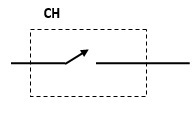
Symbol of a Chopper
Classification of Choppers
Depending on the voltage output, choppers are classified as −
- Step Up chopper (boost converter)
- Step Down Chopper(Buck converter)
- Step Up/Down Chopper (Buck-boost converter)
Step Up Chopper
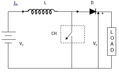
The average voltage output (Vo) in a step up chopper is greater than the voltage input (Vs). The figure below shows a configuration of a step up chopper.
Current and Voltage Waveforms
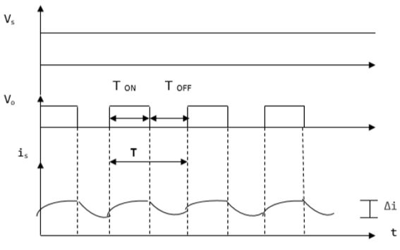
V0 (average voltage output) is positive when chopper is switched ON and negative when the chopper is OFF as shown in the waveform below.
Where
TON – time interval when chopper is ON
TOFF – time interval when chopper is OFF
VL – Load voltage
Vs – Source voltage
T – Chopping time period = TON + TOFF
Vo is given by −
$$V_{0}=frac{1}{T}int_{0}^{T_{ON}}V_{S}dt$$
When the chopper (CH) is switched ON, the load is short circuited and, therefore, the voltage output for the period TON is zero. In addition, the inductor is charged during this time. This gives VS = VL
$Lfrac{di}{dt}=V_{S},$ $frac{Delta i}{T_{ON}}=frac{V_{S}}{L}$
Hence,$Delta i=frac{V_{S}}{L}T_{ON}$
Δi = is the inductor peak to peak current. When the chopper (CH) is OFF, discharge occurs through the inductor L. Therefore, the summation of the Vs and VL is given as follows −
$V_{0}=V_{S}+V_{L},quad V_{L}=V_{0}-V_{S}$
But $Lfrac{di}{dt}=V_{0}-V_{S}$
Thus,$Lfrac{Delta i}{T_{OFF}}=V_{0}-V_{S}$
This gives,$Delta i=frac{V_{0}-V_{S}}{L}T_{OFF}$
Equating Δi from ON state to Δi from OFF state gives −
$frac{V_{S}}{L}T_{ON}=frac{V_{0}-V_{S}}{L}T_{OFF}$, $V_{S}left ( T_{ON}+T_{OFF} right )=V_{0}T_{OFF}$
$V_{0}=frac{TV_{S}}{T_{OFF}}=frac{V_{S}}{frac{left ( T+T_{ON} right )}{T}}$
This give the average voltage output as,
$$V_{0}=frac{V_{S}}{1-D}$$
The above equation shows that Vo can be varied from VS to infinity. It proves that the output voltage will always be more than the voltage input and hence, it boosts up or increases the voltage level.
Step Down Chopper
This is also known as a buck converter. In this chopper, the average voltage output VO is less than the input voltage VS. When the chopper is ON, VO = VS and when the chopper is off, VO = 0
When the chopper is ON −
$V_{S}=left ( V_{L}+V_{0} right ),quad V_{L}=V_{S}-V_{0},quad Lfrac{di}{dt}=V_{S}-V_{0},quad Lfrac{Delta i}{T_{ON}}=V_{s}+V_{0}$
Thus, peak-to-peak current load is given by,
$Delta i=frac{V_{s}-V_{0}}{L}T_{ON}$
Circuit Diagram
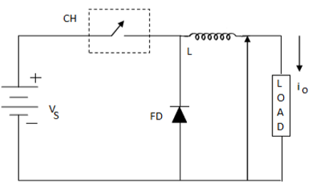
Where FD is free-wheel diode.
When the chopper is OFF, polarity reversal and discharging occurs at the inductor. The current passes through the free-wheel diode and the inductor to the load. This gives,
$$Lfrac{di}{dt}=V_{0}………………………………….left ( i right )$$
Rewritten as −$quad Lfrac{Delta i}{T_{OFF}}=V_{0}$
$$Delta i=V_{0}frac{T_{OFF}}{L}……………………………..left ( ii right )$$
Equating equations (i) and (ii) gives;
$frac{V_{S}-V_{0}}{L}T_{ON}=frac{V_{0}}{L}T_{OFF}$
$frac{V_{S}-V_{0}}{V_{0}}=frac{T_{OFF}}{T_{ON}}$
$frac{V_{S}}{V_{0}}=frac{T_{ON}-T_{OFF}}{T_{ON}}$
The above equation gives;
$$V_{0}=frac{T_{ON}}{T}V_{S}=DV_{S}$$
Equation (i) gives −
$Delta i=frac{V_{S}-DV_{S}}{L}DT$, from $D=frac{T_{ON}}{T}$
$=frac{V_{S}-left ( 1-D right )D}{Lf}$
$f=frac{1}{T}=$chopping frequency
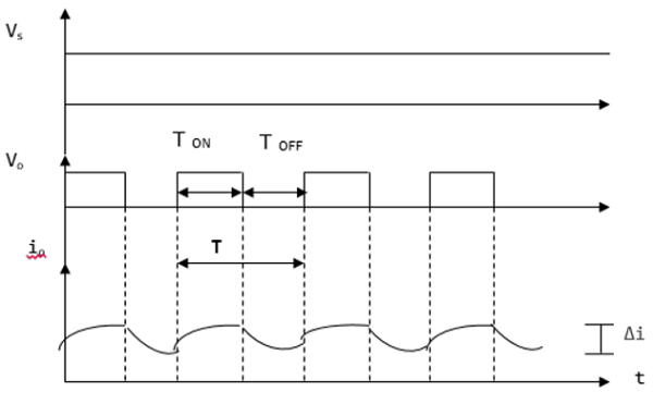
Current and Voltage Waveforms
The current and voltage waveforms are given below −
For a step down chopper the voltage output is always less than the voltage input. This is shown by the waveform below.
Step Up/ Step Down Chopper
This is also known as a buck-boost converter. It makes it possible to increase or reduce the voltage input level. The diagram below shows a buck-boost chopper.
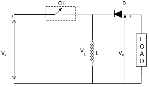
When the chopper is switched ON, the inductor L becomes charged by the source voltage Vs. Therefore, Vs = VL.
$$Lfrac{di}{dt}=V_{S}$$
$$Delta i=frac{V_{S}}{L}T_{ON}=frac{V_{S}}{L}Tfrac{T_{ON}}{T}=frac{DV_{S}}{Lf}$$
Because −
$D=frac{T_{ON}}{T}$ and $f=frac{1}{T} ………………………………………. left ( iii right )$
When the chopper is switched OFF, the inductor’s polarity reverses and this causes it to discharge through the diode and the load.
Hence,
$$V_{0}=-V_{L}$$
$$Lfrac{di}{dt}=-V_{0}$$
$Lfrac{Delta i}{T_{OFF}}=-V_{0}$, thus $Delta i=-frac{V_{0}}{L}T_{OFF}…………………………..left ( iv right )$
Evaluating equation (iii) and (iv) gives −
$frac{DV_{S}}{Lf}=-frac{V_{0}}{L}T_{OFF}$, $DV_{S}=-DV_{S}=-V_{0}T_{OFF}f$
$DV_{S}=-V_{0}frac{T-T_{ON}}{T}=-V_{0}left ( 1-frac{T_{ON}}{T} right )$, $V_{0}=-frac{DV_{S}}{1-D}$
Because $D=frac{T_{ON}}{T}=frac{T-T_{OFF}}{1-D}$
This gives,
$V_{0}=frac{DV_{S}}{1-D}$
D can be varied from 0 to 1. When, D = 0; VO = 0
When D = 0.5, VO = VS
When, D = 1, VO = ∞.
Hence, in the interval 0 ≤ D ≤ 0.5, output voltage varies in the range 0 ≤ VO < VS and we get step down or Buck operation. Whereas, in the interval 0.5 ≤ D ≤ 1, output voltage varies in the range VS ≤ VO ≤ ∞ and we get step up or Boost operation.
Power Electronics – Control Methods
In a converter, there are two basic methods of control used to vary the output voltage. These are −
- Time ratio control
- Current limit control
Time Ratio Control
In time ratio control, a constant k given by $frac{T_{ON}}{T}$ is varied. The constant k is called duty ratio. Time ratio control can be achieved in two ways −
Constant Frequency
In this control method, the frequency (f = 1/T0N) is kept constant while the ON time T is varied. This is referred to as pulse width modulation (PWM).
Variable Frequency
In variable frequency technique, the frequency (f = 1/T) is varied while the ON time T is kept constant. This is referred to as the frequency modulation control.
Current Limit Control
In a DC to DC converter, the value of the current varies between the maximum as well as the minimum level for continuous voltage. In this technique, the chopper (switch in a DC to DC converter) is switched ON and then OFF to ensure that current is kept constant between the upper and lower limits. When the current goes beyond the maximum point, the chopper goes OFF.
While the switch is at its OFF state, current freewheels via the diode and drops in an exponential manner. The chopper is switched ON when the current reaches the minimum level. This method can be used either when the ON time T is constant or when the frequency (f=1/T).
Power Electronics – Resonant Switching
Resonant switch converters refers to converters that have inductor and capacitor (L-C) networks and whose current and voltage waveforms vary in a sinusoidal manner during each period of switching. There are various resonant switch converters −
- Resonant DC to DC converters
- DC to AC inverters
- Resonant AC inverters to DC converters
In this tutorial, we will focus on Resonant DC to DC converters
Resonant DC to DC Converters
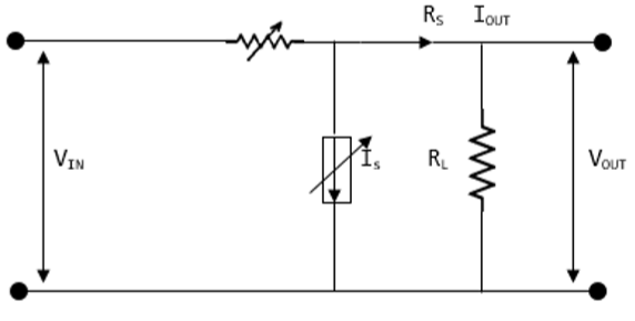
The concept of switch mode power supply (SMPS) is explained below using a DC to DC converter. The load is given a constant voltage supply (VOUT) that is obtained from a primary source of voltage supply VIN. The value of VOUT is regulated by varying resistor in series (RS) or the current source connected in shunt (IS). By controlling VOUT through varying IS and ensuring RS is kept constant, a considerable amount of power is lost in the converter.
Switched Mode Power Supply (SMPS)
An SMPS (switched mode power supply) refers to an electronic device that uses a switching regulator for the purpose of converting electrical power in an efficient manner. SMPS takes power from the main power lines and transfers it to a load. For example, a computer while ensuring the voltage and current characteristics are converted.
The difference between an SMPS and a linear supply of power is that the former keeps switching ON and OFF during low dissipation and uses less time during high dissipation regions. This ensures less energy is wasted. Actually, an SMPS does not dissipate any power.
The size of an SMPS is smaller and very light, compared to a normal linear supply power device of the same size and shape.

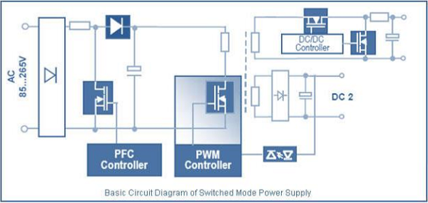
The figure below shows the circuit diagram for an SMPS. When the switching frequency is varied, the stored energy can be varied for each cycle and hence the voltage output is varied.
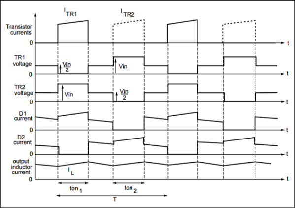
The waveforms below are for a half bridge converter also known as a push-pull. It is used in applications utilizing high power. The input voltage is halved as indicated in the waveform.
DC to DC Converters Solved Example
A step up chopper has an input voltage of 150V. The voltage output needed is 450V. Given, that the thyristor has a conducting time of 150μseconds. Calculate the chopping frequency.
Solution −
The chopping frequency (f)
$f=frac{1}{T}$
Where T – Chopping time period = $T_{ON}+T_{OFF}$
Given − $V_{S}=150V$$V_{0}=450V$ $T_{ON}=150mu sec$
$V_{0}=V_{Sleft ( frac{T}{T-T_{ON}} right )}$
$450=150frac{T}{T-150^{-6}}$ $T=225mu sec$
Therfore, $f=frac{1}{225ast 10^{-6}}=4.44KHz$
The new voltage output, on condition that the operation is at constant frequency after the halving the pulse width.
Halving the pulse width gives −
$$T_{ON}=frac{150times 10^{-6}}{2}=75mu sec$$
The frequency is constant thus,
$$f=4.44KHz$$
$$T=frac{1}{f}=150mu sec$$
The voltage output is given by −
$$V_{0}=V_{S}left ( frac{T}{T-T_{ON}} right )=150times left ( frac{150times 10^{-6}}{left ( 150-75 right )times 10^{-6}} right )=300Volts$$
Power Electronics – Types of Inverters
An inverter refers to a power electronic device that converts power in DC form to AC form at the required frequency and voltage output.
Inverters are classified into two main categories −
-
Voltage Source Inverter (VSI) − The voltage source inverter has stiff DC source voltage that is the DC voltage has limited or zero impedance at the inverter input terminals.
-
Current Source Inverter (CSI) − A current source inverter is supplied with a variable current from a DC source that has high impedance. The resulting current waves are not influenced by the load.
Single Phase Inverter
There are two types of single phase inverters − full bridge inverter and half bridge inverter.
Half Bridge Inverter
This type of inverter is the basic building block of a full bridge inverter. It contains two switches and each of its capacitors has a voltage output equal to $frac{V_{dc}}{2}$. In addition, the switches complement each other, that is, if one is switched ON the other one goes OFF.
Full Bridge Inverter
This inverter circuit converts DC to AC. It achieves this by closing and opening the switches in the right sequence. It has four different operating states which are based on which switches are closed.
Three Phase Inverter
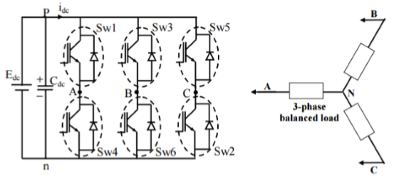
A three-phase inverter converts a DC input into a three-phase AC output. Its three arms are normally delayed by an angle of 120° so as to generate a three-phase AC supply. The inverter switches each has a ratio of 50% and switching occurs after every T/6 of the time T (60° angle interval). The switches S1 and S4, the switches S2 and S5 and switches S3 and S6 complement each other.
The figure below shows a circuit for a three phase inverter. It is nothing but three single phase inverters put across the same DC source. The pole voltages in a three phase inverter are equal to the pole voltages in single phase half bridge inverter.
The two types of inverters above have two modes of conduction − 180° mode of conduction and 120° mode of conduction.
180° mode of conduction
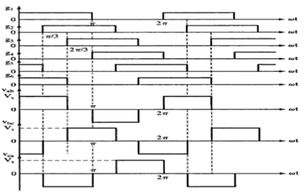
In this mode of conduction, every device is in conduction state for 180° where they are switched ON at 60° intervals. The terminals A, B and C are the output terminals of the bridge that are connected to the three-phase delta or star connection of the load.
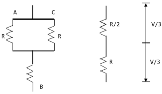
The operation of a balanced star connected load is explained in the diagram below. For the period 0° − 60° the points S1, S5 and S6 are in conduction mode. The terminals A and C of the load are connected to the source at its positive point. The terminal B is connected to the source at its negative point. In addition, resistances R/2 is between the neutral and the positive end while resistance R is between the neutral and the negative terminal.
|
The load voltages are gives as follows; VAN = V/3, VBN = −2V/3, VCN = V/3 |
The line voltages are given as follows; VAB = VAN − VBN = V, VBC = VBN − VCN = −V, VCA = VCN − VAN = 0 |
Waveforms for 180° mode of conduction
120° mode of conduction
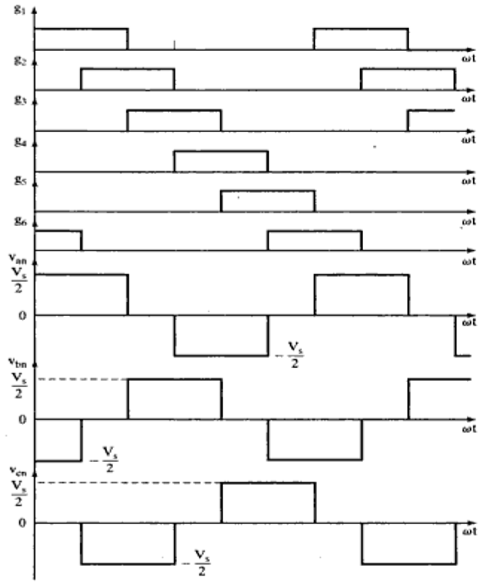
In this mode of conduction, each electronic device is in a conduction state for 120°. It is most suitable for a delta connection in a load because it results in a six-step type of waveform across any of its phases. Therefore, at any instant only two devices are conducting because each device conducts at only 120°.
The terminal A on the load is connected to the positive end while the terminal B is connected to the negative end of the source. The terminal C on the load is in a condition called floating state. Furthermore, the phase voltages are equal to the load voltages as shown below.
Phase voltages = Line voltages
VAB = V
VBC = −V/2
VCA = −V/2
Waveforms for 120° mode of conduction
Power Electronics – Pulse Width Modulation
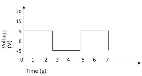
PWM is a technique that is used to reduce the overall harmonic distortion (THD) in a load current. It uses a pulse wave in rectangular/square form that results in a variable average waveform value f(t), after its pulse width has been modulated. The time period for modulation is given by T. Therefore, waveform average value is given by
$$bar{y}=frac{1}{T}int_{0}^{T}fleft ( t right )dt$$
Sinusoidal Pulse Width Modulation
In a simple source voltage inverter, the switches can be turned ON and OFF as needed. During each cycle, the switch is turned on or off once. This results in a square waveform. However, if the switch is turned on for a number of times, a harmonic profile that is improved waveform is obtained.
The sinusoidal PWM waveform is obtained by comparing the desired modulated waveform with a triangular waveform of high frequency. Regardless of whether the voltage of the signal is smaller or larger than that of the carrier waveform, the resulting output voltage of the DC bus is either negative or positive.
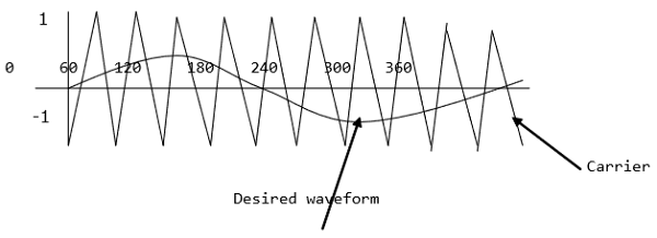
The sinusoidal amplitude is given as Am and that of the carrier triangle is give as Ac. For sinusoidal PWM, the modulating index m is given by Am/Ac.
Modified Sinusoidal Waveform PWM
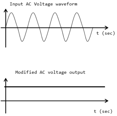
A modified sinusoidal PWM waveform is used for power control and optimization of the power factor. The main concept is to shift current delayed on the grid to the voltage grid by modifying the PWM converter. Consequently, there is an improvement in the efficiency of power as well as optimization in power factor.
Multiple PWM
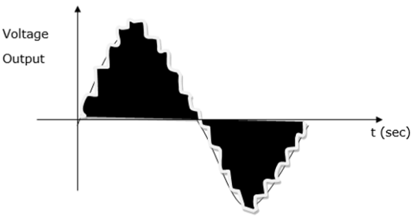
The multiple PWM has numerous outputs that are not the same in value but the time period over which they are produced is constant for all outputs. Inverters with PWM are able to operate at high voltage output.

The waveform below is a sinusoidal wave produced by a multiple PWM
Voltage and Harmonic Control
A periodic waveform that has frequency, which is a multiple integral of the fundamental power with frequency of 60Hz is known as a harmonic. Total harmonic distortion (THD) on the other hand refers to the total contribution of all the harmonic current frequencies.
Harmonics are characterized by the pulse that represent the number of rectifiers used in a given circuit. It is calculated as follows −
$$h=left ( ntimes P right )+1 quad or quad -1$$
Where n − is an integer 1, 2, 3, 4….n
P − Number of rectifiers
It is summarized in the table below −
|
Harmonic |
Frequency |
| 1st | 60 Hz |
| 2nd | 120 Hz |
| 3rd | 180Hz |
| 4th | 240Hz |
|
5th . . 49th |
300Hz . . 2940Hz |
Harmonics have an impact on the voltage and current output and can be reduced using isolation transformers, line reactors, redesign of power systems and harmonic filters.
Series Resonant Inverter
A resonant inverter is an electrical inverter whose operation is based on oscillation of resonant current. Here, the switching device and the resonanting component are connected in series to each other. As a result of the natural features of the circuit, the current passing through the switching device drops to zero.
This type of inverter yields a sinusoidal waveform at very high frequencies in the range of 20kHz-100kHz. It is therefore, most suitable for applications that demand a fixed output such as induction heating and flourescent lighting. It is usually small in size because its switching frequency is high.
A resonant inverter has numerous configurations and thus it is categorized into two groups −
- Those with unidirectional switches
- Those with bidirectional switches
Power Electronics – Inverters Solved Example
A single phase half bridge inverter has a resistance of 2.5Ω and input DC voltage of 50V. Calculate the following −
Solution −
a. The RMS voltage occurring at the fundamental frequency
$E_{1RMS}=0.9times 50V=45V$
b. The power Output
RMS output voltage $E_{ORMS}=E=50V$
Output power $=E^{2}/R=left ( 50right )^{2}/2.5=1000W$
c. Peak current and average current
Peak current $I_{p}=E_{0}/R=50/2.5=20A$
Average current$=I_{p}/2=20/2=10A$
d. Harmonic RMS voltage
$E_{n}=left { left ( E_{ORMS} right )^{2}-left ( E_{1RMS} right )^{2} right }^{0.5}=left [ 50^{2} -45^{2}right ]^{0.5}=21.8V$
e. Total harmonic distortion
$E_{n}/E_{1RMS}=21.8/45=0.48times 100%=48%$
Single Phase AC Voltage Controllers
A single-phase AC controller (voltage controller) is used to vary the value of the alternating voltage after it has been applied to a load circuit. A thyristor is also placed between the load and the constant source of AC voltage.
The root mean square alternating voltage is regulated by changing the thyristor triggering angle. In the case of phase control, the thyristors are employed as switches to establish a connection from the AC input supply to the load circuit during each input cycle. For every positive input voltage, chopping occurs and voltage is reduced.
Circuit Diagram with a Resistive Load

During half part of the cycle, the thyristor switch is turned ON to enable the voltage input to appear across the load. This is followed by the OFF state during the last half cycle so as to disconnect the load from the source voltage.
When the triggering angle α is controlled, the RMS value of the voltage on the load is also controlled. The triggering angle α is therefore, defined as the value of ωt at which the thyristor switches ON.
Multistage Sequence Control of AC Converter
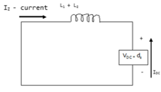
When two or more sequence control stages are connected, it is possible to have an improvement in power factor and further reduction in THD (total harmonic distortion). An n-stage sequence control converter has n windings in the transformer secondary part with each rated es/n (the source voltage).
When two AC converters are placed parallel to each other, the zero sequence way is created. A little difference between the two converters causes a great zero sequence in circulating current. The diagram below shows the parallel system of a converter. The direction of the current is anti-clockwise with respect to that of the voltage system.
Power Electronics – Cycloconverters
A cycloconverter refers to a frequency changer that can to change AC power from one frequency to AC power at another frequency. This process is known as AC-AC conversion. It is mainly used in electric traction, AC motors having variable speed and induction heating.
A cycloconverter can achieve frequency conversion in one stage and ensures that voltage and the frequencies are controllable. In addition, the need to use commutation circuits is not necessary because it utilizes natural commutation. Power transfer within a cycloconverter occurs in two directions (bidirectional).
A major problem with cycloconverters is that when it is operating at small currents, there are inefficiencies created with firing delay. Furthermore, operations are only smooth at frequencies that are not equal half frequency input values. This is true because a cycloconverter is an AC- AC converter that is phase controlled. Therefore, for it to give the required AC output voltage, it has to do a selection of the voltage input segments by applying line (natural) commutation. This explains why the output frequency is lower than the frequency input.
Harmonics in a cycloconverter are mainly affected by methods of control, overlap effect, the number of pulses in a given cycle, operation mode and mode of conduction.
There are two types of cycloconverters−
-
Step Up cycloconverter − These types use natural commutation and give an output at higher frequency than that of the input.
-
Step Down cycloconverter − This type uses forced commutation and results in an output with a frequency lower than that of the input.
Cycloconverters are further classified into three categories −
-
Single phase to single-phase − This type of cycloconverter has two full wave converters connected back to back. If one converter is operating the other one is disabled, no current passes through it.
-
Three-phase to single-phase − This cycloconverter operates in four quadrants that is (+V, +I) and (−V, −I) being the rectification modes and (+V, −I) and (−V, +I) being the inversion modes.
-
Three-phase to three-phase − This type of cycloconverter is majorly used in AC machine systems that are operating on three phase induction and synchronous machines.
Power Electronics – Integral Cycle Control
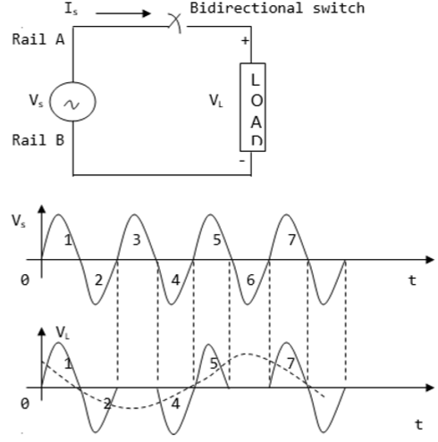
Integral cycle controllers are converters with the ability to perform direct switching without losses. The process directly converts AC to AC without having to perform the intermediate processes of AC to DC then DC to AC.
The basic integral control cycle is sinusoidal in nature. It operates by combining and eliminating higher frequency half cycles from AC input. The controllers are normally, turned ON of OFF during half cycles where the voltage input is at zero since only the full or half cycles are utilized. Therefore, integral cycle circuits achieve switching at zero voltage without requiring a resonant circuit.
The diagram below shows a simple integral cycle controller. It contains a load and a power switch, which performs the direct conversion. This diagram shows the conversion of source frequency from a factor of three to one.
Power Factor Control
Power factor control, also known as correction of power factor, is the process of reducing the amount of reactive power. The power electronic device used in this case is called a power factor controller (PFC). From the power triangle (which comprises reactive, true and apparent power), the reactive power is at right angle (90°) to the true power and is used to energize the magnetic field. Although reactive power does not have a real value in electronic equipment, the bill for electricity comprises real and reactive power costs. This makes it necessary to have power factor controllers in electronic devices.
Power factor (k) is defined as the ratio of the real power (in kW) to the reactive power (in kVAr). Its value ranges from 0 to 1. If a device has a power factor of 0.8 and above, it is said to be using power efficiently. Incorporating a PFC ensures the power factor ranges from 0.95 to 0.99. Power factor controllers are mainly in industrial equipment to minimize reactive power generated by fluorescent lighting and electric motors.
To ensure power factor is improved without causing harmonic distortion, the conventional capacitors should not be used. Instead, filters (combination of capacitors and reactors) for harmonic suppression are used. The figure below shows a harmonic filter.
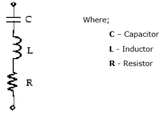
The above type of harmonic filter is referred to as a single tuned filter. A quality factor Q of this filter is defined as quality factor of its reactance (XL) at Q (tuning frequency) where Q is given by (nXL/R).
Power Electronics – Matrix Converters
A matrix converter is defined as a converter with a single stage of conversion. It utilizes bidirectional controlled switch to achieve automatic conversion of power from AC to AC. It provides an alternative to PWM voltage rectifier (double sided).
Matrix converters are characterized by sinusoidal waveforms that show the input and output switching frequencies. The bidirectional switches make it possible to have a controllable power factor input. In addition, the lack of DC links ensures it has a compact design. The downside to matrix converters is that they lack bilateral switches that are fully controlled and able to operate at high frequencies. Its voltage ratio that is output to input voltage is limited.
There are three methods of matrix converter control −
- Space vector modulation
- Pulse width modulation
- Venturi – analysis of function transfer
The Matrix Converter Circuit
The diagram given below shows a single-phase matrix converter.
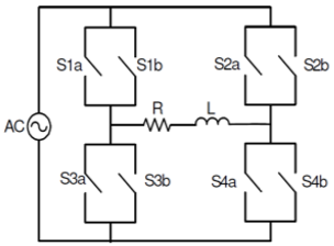
It contains four bi-directional switches with each switch having the ability to conduct in both forward blocking and reverse voltage.
Space Vector Modulation (SVM)
SVM refers to a method of algorithm used to control the PWM. It creates AC waveforms that drive AC motors at various speeds. In the case of a three-phase inverter having DC supply power, its three main legs at the output are connected to a 3-phase motor.
The switches are under control to ensure that no two switches in the same leg are ON at the same time. Simultaneous ON states could result in the DC supply shorting. This leads to eight switching vectors where two are zero and six are active vectors for switching.
AC to DC Converters Solved Example
A single-phase AC voltage converter has the following details −
ON time = 6 min, OFF time = 4 min, frequency = 50Hz, and
Voltage source Vo = 110V
Calculate the following.
Triggering angle α
Solution −
$T=2times left ( T_{ON}+T_{OFF} right )$ but $f=50Hz,$ $T=2times left ( 6+4 right )=20mins$
$360^{circ}=20min,$ $1min=18^{circ}$
Therefore, $T_{OFF}=4min$
Then,
$$alpha =frac{4}{0.1}times 1.8=72^{circ}$$
Voltage Output
Solution −
$$V_{0}=left ( V_{S}times D right ),quad where quad D=frac{T_{ON}}{T_{ON}+T_{OFF}}=frac{6}{10}=0.6$$
$$T_{ON}=6min,quad T_{OFF}=4 min,quad V_{S}=110V$$
$$V_{0}left ( Voltage Output right )=V_{S}times D=110times 0.6=66Volts$$
Learning working make money